
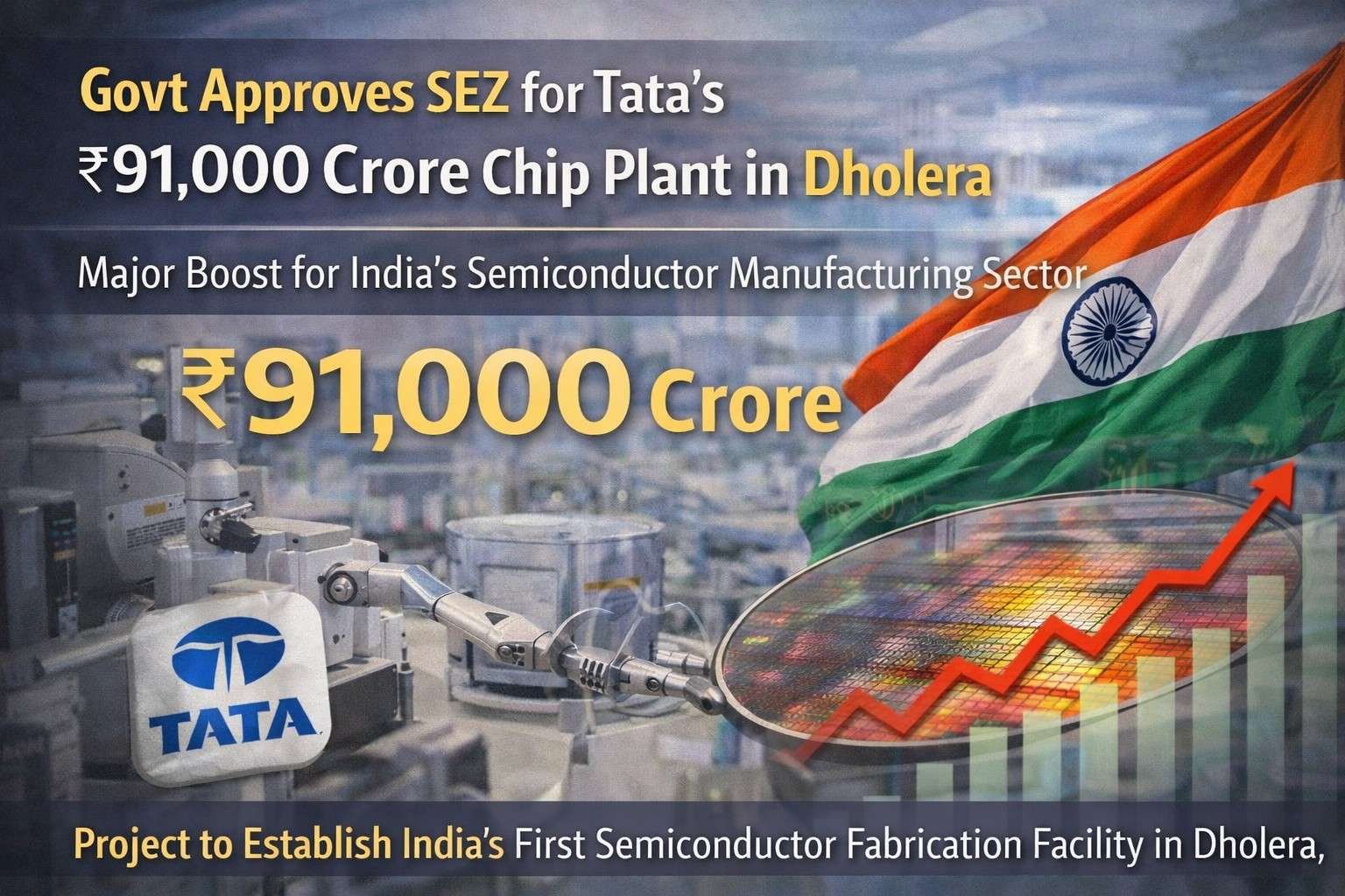
In a significant move to strengthen India’s semiconductor ecosystem, the government has approved the establishment of a Special Economic Zone (SEZ) for Tata Semiconductor Manufacturing in Dholera, Gujarat. The project, with a massive proposed investment of ₹91,000 crore, is set to house India’s first semiconductor fabrication (chip fab) facility.
A Major Boost to India’s Chip Ambitions
The approval marks a key milestone in India’s efforts to become a global hub for semiconductor manufacturing. The SEZ will focus on electronic hardware and software production, including IT and ITeS services.
The proposal was cleared by the Board of Approval, the apex body for SEZ-related decisions, chaired by the Commerce Secretary. Following this, the Department of Commerce officially notified the SEZ on April 9.
Key Features of the Project
- Location: Dholera, Gujarat
- Investment: ₹91,000 crore
- Area: 66.16 hectares
- Employment Generation: Around 21,000 jobs
- Purpose: Semiconductor fabrication and related ecosystem development
This project is expected to reduce India’s dependence on imported chips and enhance domestic manufacturing capabilities in high-tech sectors.
Policy Support and Reforms
To promote semiconductor and electronics manufacturing, the government has introduced key policy changes:
- Minimum land requirement for SEZs in this sector reduced from 50 hectares to 10 hectares
- Faster approvals and simplified regulatory processes
- Strong push through targeted schemes and incentives
These reforms aim to attract large-scale investments and accelerate infrastructure development in the sector.
Growing Semiconductor Ecosystem
The Tata project is part of a broader push by the government to build a robust semiconductor ecosystem. So far, five new SEZs have been approved in this space, including:
- CG Semi (₹2,150 crore)
- Kaynes Semicon (₹681 crore)
- Micron Semiconductor Technology India (₹13,000 crore)
- Hubballi Durable Goods Cluster (₹100 crore)
Additionally, the government has approved 10 semiconductor projects with a total investment of around ₹1.6 lakh crore, including:
- 2 semiconductor fabrication units (fabs)
- 8 packaging and related units
India Semiconductor Mission 2.0
In the Union Budget 2026, the government launched India Semiconductor Mission 2.0, aimed at:
- Developing semiconductor equipment and materials
- Promoting full-stack chip design with Indian intellectual property
- Strengthening supply chains
To support this mission, the government has increased the outlay to ₹40,000 crore, building on earlier initiatives like the Electronics Components Manufacturing Scheme (2025).
Conclusion
The approval of Tata’s semiconductor SEZ in Dholera represents a transformative step in India’s industrial and technological journey. With strong policy backing, rising investments, and a clear strategic vision, India is steadily positioning itself as a key player in the global semiconductor value chain.