

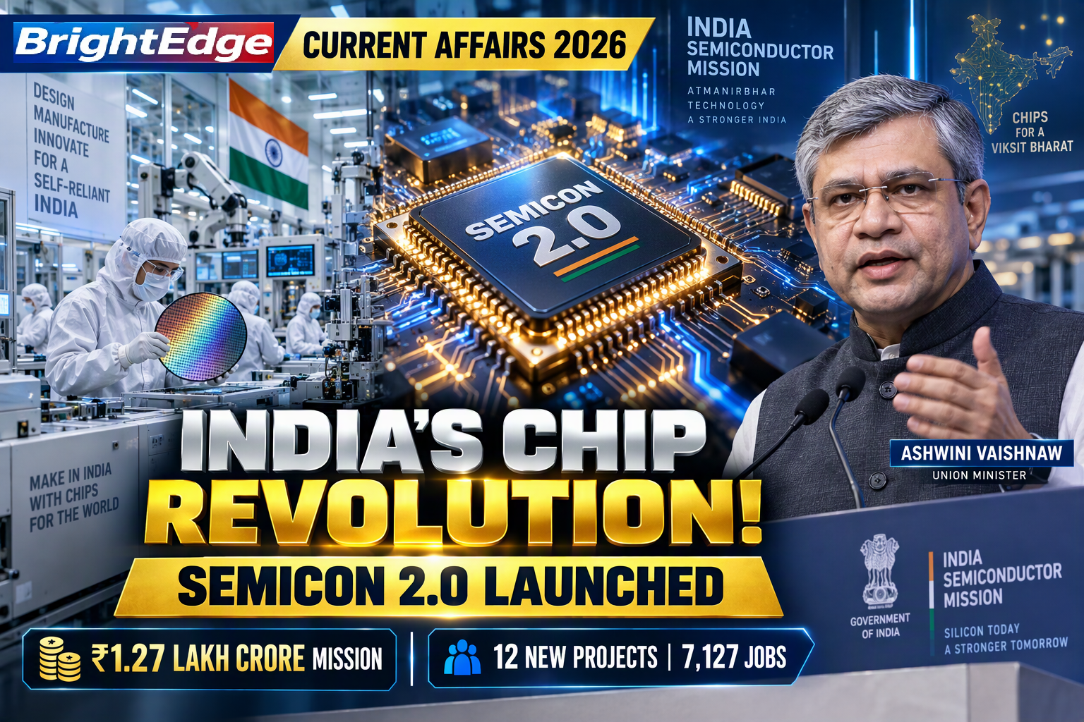
Union Minister for Electronics and Information Technology, Railways and Information & Broadcasting Ashwini Vaishnaw launched the Semicon 2.0 Web Application Portal on November 6, 2026, marking a major step towards strengthening India’s semiconductor and electronics manufacturing ecosystem.
The newly launched portal allows companies to submit applications under three strategic pillars of the Semicon India Programme: semiconductor machines and materials, setting up additional fabrication facilities (fabs), and strengthening the Assembly, Testing, Marking and Packaging (ATMP) and Outsourced Semiconductor Assembly and Test (OSAT) industries.
The Union Cabinet has approved Semicon 2.0 with a financial outlay of ₹1,27,500 crore under the India Semiconductor Mission.
Alongside the portal launch, the government announced 12 additional approved applicants under the Electronics Components Manufacturing Scheme (ECMS), involving a projected investment of ₹7,503 crore.
Semicon 2.0 Portal Launched by Ashwini Vaishnaw
On November 6, 2026, Ashwini Vaishnaw officially launched the Semicon 2.0 Web Application Portal in New Delhi.
The portal is designed to facilitate applications from companies interested in participating in India’s semiconductor manufacturing ecosystem.
Initially, applications have been opened for three of the programme’s six strategic pillars:
- Pillar 2: Machines and Materials.
- Pillar 3: Setting Up More Semiconductor Fabrication Facilities.
- Pillar 4: Strengthening ATMP and OSAT Industries.
These three pillars focus on developing critical manufacturing infrastructure and expanding India’s domestic semiconductor supply chain.
The launch represents an important transition from policy announcements towards the implementation and expansion of semiconductor manufacturing projects.
What Is Semicon 2.0?
- Semicon 2.0 is the next phase of India’s semiconductor development strategy under the India Semiconductor Mission (ISM).
- It aims to establish a comprehensive semiconductor ecosystem covering chip design, manufacturing, packaging, research, advanced equipment, raw materials and skilled manpower.
- The programme builds on the achievements of the first phase of the Semicon India Programme, which focused on establishing the foundation for domestic semiconductor manufacturing.
- With a financial outlay of ₹1,27,500 crore, Semicon 2.0 aims to strengthen India’s position in the global semiconductor value chain.
Six Strategic Pillars of Semicon 2.0
The programme is structured around six major pillars:
1. Design of Chips
Promoting semiconductor chip design capabilities and supporting innovation in advanced chip technologies.
2. Machines and Materials
Developing domestic manufacturing capabilities for semiconductor equipment, specialised machinery, chemicals and materials.
3. Setting Up More Fabs
Encouraging the establishment of additional semiconductor fabrication facilities in India to increase domestic chip production capacity.
4. Strengthening ATMP/OSAT Industry
Expanding semiconductor assembly, testing, marking and packaging capabilities, which are essential stages in semiconductor manufacturing.
5. Research and Development
Promoting innovation, advanced semiconductor technologies and research activities to strengthen India’s technological capabilities.
6. Talent Development
Developing a skilled workforce of semiconductor engineers, researchers, designers and manufacturing professionals.
Applications Open for Three Major Pillars
- The newly launched Semicon 2.0 portal has opened applications for Pillars 2, 3 and 4.
- These areas are particularly important because semiconductor manufacturing requires sophisticated machinery, specialised materials, fabrication infrastructure and advanced packaging facilities.
- The government intends to attract technologically capable companies and encourage domestic and international investment in these strategic sectors.
- The focus on machines, materials and advanced packaging is expected to deepen India’s manufacturing capabilities beyond semiconductor chip design and assembly.
12 New Projects Approved Under Electronics Components Manufacturing Scheme
These projects involve:
| Particular | Details |
|---|---|
| Newly Approved Applicants | 12 |
| Projected Investment | ₹7,503 crore |
| Expected Production | ₹39,045 crore |
| Direct Employment | 7,127 jobs |
| Product Segments Covered | 10 |
| States Covered | 7 |
The newly approved projects cover several important electronics manufacturing segments, including:
- Multi-layer Printed Circuit Boards (PCBs).
- Relays.
- Heat sinks.
- Specialty ceramics.
- Copper foil.
- Anode materials.
- Cathode active materials.
- Polypropylene film.
- Camera rims.
- Capital goods and their parts.
The approvals include first-time projects under ECMS for copper foil, cathode active material and specialty ceramics.
The projects will be established across Gujarat, Karnataka, Madhya Pradesh, Maharashtra, Punjab, Tamil Nadu and Uttar Pradesh.
ECMS: Total Approved Investments Reach ₹77,051 Crore
With the latest 12 approvals, the total number of approved applications under the Electronics Components Manufacturing Scheme has reached 118.
The cumulative achievements include:
| Particular | Total |
|---|---|
| Approved Applications | 118 |
| Products Covered | 34 |
| States Covered | 16 |
| Expected Investment | ₹77,051 crore |
| Projected Production | ₹5,73,146 crore |
| Expected Direct Employment | 81,755 |
Approximately 50% of the units approved under the scheme belong to the Micro, Small and Medium Enterprises (MSME) sector.
This highlights the growing participation of smaller manufacturing enterprises in India’s electronics supply chain.
The scheme is expected to strengthen domestic production, increase value addition, reduce import dependence and generate employment opportunities.
India’s Progress Under Semicon India Programme 1.0
The first phase of the Semicon India Programme established the foundation for India’s semiconductor manufacturing ecosystem.
According to the Ministry of Electronics and Information Technology:
- 12 semiconductor projects were approved across six states.
- Cumulative investments exceeded ₹1.64 lakh crore.
- Five of the 12 projects had commenced commercial production by October 2026.
- 105 startups received access to Electronic Design Automation (EDA) tools.
- 24 startups received funding support.
- 15 startups secured venture capital funding.
- 332 institutions received EDA tools under the Chips to Startup (C2S) Programme.
- Approximately 70,000 students received training.
These achievements demonstrate the expansion of India’s semiconductor design, research and manufacturing ecosystem.
India’s Semiconductor Vision: Reducing Import Dependence
Semiconductors are essential components used in modern electronic devices and advanced technologies.
They are widely used in:
- Smartphones and computers.
- Automobiles and electric vehicles.
- Artificial intelligence systems.
- Telecommunications equipment.
- Defence and aerospace technologies.
- Medical equipment.
- Industrial automation.
- Consumer electronics.
India’s semiconductor strategy aims to reduce dependence on imported chips and critical electronic components by developing domestic manufacturing capabilities.
The government is also focusing on attracting major equipment manufacturers and companies operating in specialised chemicals and gases.
Under Semicon 2.0, the government aims to attract at least three major equipment manufacturers and five companies in the chemicals and gases sectors.
These industries are essential for developing a complete semiconductor manufacturing ecosystem.
Significance of Semicon 2.0 for India
The launch of the Semicon 2.0 portal is significant for India’s economic and technological development.
1. Boost to Make in India
The programme will encourage domestic semiconductor and electronics manufacturing.
2. Reduced Import Dependence
Developing domestic capabilities in chips, materials and equipment can reduce India’s dependence on foreign supply chains.
3. Employment Generation
Semiconductor manufacturing requires engineers, technicians, researchers and skilled production workers, creating opportunities for employment.
4. Technology Development
Investment in research and development will help India strengthen its capabilities in advanced semiconductor technologies.
5. Global Competitiveness
The initiative aims to position India as an important destination for semiconductor investment and manufacturing.
6. MSME Participation
Greater participation of MSMEs can strengthen the domestic electronics supply chain and encourage entrepreneurship.
Click here to read: Sardar Vallabhbhai Patel: The Iron Man Who United India
Click here to read: Ashoke Sen Wins Oskar Klein Medal 2026: First Indian Physicist